
Blog
The difference between a MOSFET and a power MOSFET

 4 Nov 2026
 8 min read
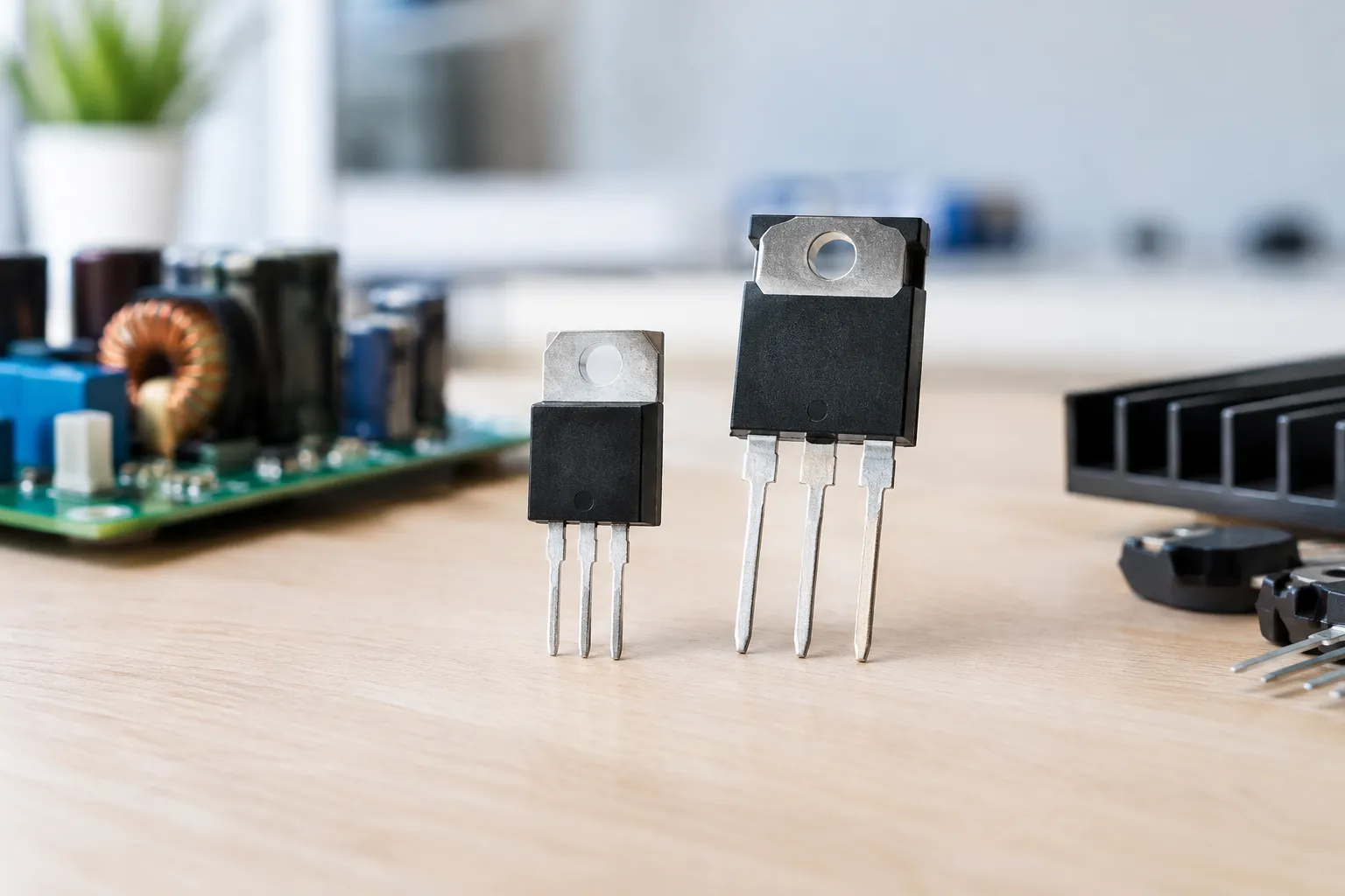
The difference between a MOSFET and a power MOSFET is mainly a matter of design and intended use: a power MOSFET is built and packaged for switching higher voltage or current, while using the same basic transistor principle. To compare them, separate power handling from power dissipation and examine the conditions behind each datasheet rating.
Is a power MOSFET different from a standard MOSFET?

A power MOSFET is a MOSFET designed for power switching, not a different kind of transistor in principle. Its structure, package, and thermal path are adapted to its intended voltage, current, and heat loads.
What does “power” mean in this context?
Here, “power” describes the electrical and thermal demands of the application, not a separate operating principle. A MOSFET controls current through a channel using an electric field; a power MOSFET is designed to perform that function in circuits where voltage, current, and heat dissipation are significant design constraints.
That distinction helps resolve the query “what is the difference between MOSFET and power MOSFET?” The answer is not that one has power and the other does not. Rather, the term “power MOSFET” identifies a MOSFET intended for power applications. A signal-level MOSFET may suit low-power control, while a power MOSFET may be selected for a switching stage that must handle higher electrical loads. The device’s actual limits still depend on its datasheet and the circuit.
“Power MOSFET” also should not be confused with the phrase “MOSFET power.” That phrase can refer to the power handled by a device or to power dissipated as heat. Those are different quantities: power transferred through a circuit is not automatically the same as heat generated inside the transistor.
The product category is not a substitute for comparing the particular device against the design. For example, engineers evaluating high-voltage conversion may compare MOSFET options with other power components, such as High Voltage Silicon Carbide Diodes, according to each component’s role in the circuit.
How do power MOSFETs handle higher voltage and current?
Power MOSFETs use device structures and packages intended to support power switching, but voltage capability, current capability, and heat removal remain specific to each part and its operating conditions.
A power device’s layout, die, and package help manage electrical stress and move heat away from the junction. The package matters because the device must connect electrically and transfer heat into its mounting or cooling arrangement. A package that does not fit the board, assembly, or thermal design is not a suitable choice merely because its electrical category sounds right.
Voltage and current ratings also answer different questions. A voltage rating sets a limit on drain-to-source voltage under specified conditions; a current rating is tied to the datasheet’s thermal and electrical assumptions. Neither means that the MOSFET can continuously operate at its maximum voltage and maximum current simultaneously in an arbitrary circuit.
For a high-voltage SiC selection, the specification must match the actual requirement across voltage rating, on-resistance, and package. If a requirement calls for a particular combination, a device that matches only the voltage but not the resistance or package is not an equivalent fit. Check the device datasheet and package details rather than inferring suitability from the words “power MOSFET” or “SiC.”
How do their switching and conduction characteristics compare?

Both standard and power MOSFETs conduct and switch according to their device characteristics; the useful comparison is how those characteristics fit the circuit’s current, voltage, switching frequency, and thermal limits.
When a MOSFET is on, its channel resistance contributes to conduction loss. For a given current, higher on-resistance generally means more heat from conduction. But the stated resistance is measured under specified conditions, including gate-to-source voltage and temperature, so it should not be treated as a fixed value in every design.
During switching, voltage and current can overlap for a short time, producing switching loss. The amount depends on factors including the switching waveform, gate drive, load, and switching frequency. A device with low on-resistance is not automatically the best choice if its switching behavior or drive requirements do not suit the application.
These tradeoffs apply to silicon and SiC MOSFETs, but the relevant comparison is between the actual parts and operating conditions, not a broad category label. Engineers assessing candidates should review gate-charge and switching information alongside on-resistance and voltage limits. Our guide to MOSFET ratings explains how to read these figures in the context of circuit requirements.
How should you interpret a power MOSFET’s ratings and dissipation?

Treat a power MOSFET’s ratings as limits defined by test conditions, not as a promise that the device can sustain every listed maximum at once. Check voltage, current, losses, and thermal conditions together.
The power dissipation of a MOSFET is the heat generated inside it, mainly through conduction and switching losses. The datasheet’s maximum power-dissipation figure depends on the specified temperature and thermal path. If the actual mounting or cooling is less effective than the test setup, the usable dissipation can be lower.
A practical interpretation starts with the circuit’s worst relevant operating conditions. Determine the maximum drain-to-source voltage, current waveform, switching frequency, and gate-drive conditions. Then estimate the heat generated and assess whether the device can transfer that heat to its surroundings while remaining within its temperature limits.
The phrase “what is MOSFET power?” can point to more than one question. It may ask how much power a MOSFET can switch, or how much power it dissipates. The first concerns the circuit load and device limits; the second concerns heat generated in the device. Keeping those meanings separate prevents a headline rating from being mistaken for a direct measure of practical circuit capability.
For a broader view of how device operation connects to circuit-level choices, read MOSFET power selection.
Why do datasheet test conditions matter?
Datasheet conditions define the circumstances under which a rating or characteristic was measured, so a number is useful only when those conditions resemble the intended circuit closely enough.
Check the listed case or ambient temperature, gate voltage, pulse duration, mounting assumptions, and test circuit. For example, an on-resistance value specified at one gate voltage should not be assumed at a different drive voltage. Likewise, a pulsed current rating does not establish a continuous-current limit.
Maximum ratings are boundaries, not recommended operating targets. A design should account for expected variation in supply, load, temperature, and switching behavior, then preserve appropriate margin according to the system requirements. If the package or heatsink arrangement differs from the datasheet setup, reassess the thermal path rather than carrying over the published dissipation figure unchanged.
The IEC standard for field-effect transistors covers classifications and requirements for devices including MOSFETs. For practical design work, the individual manufacturer datasheet remains the place to check a specific device’s ratings, characteristics, and stated test conditions.
How do you estimate operating temperature and losses?
Estimate conduction and switching losses under the circuit’s operating conditions, then use the device’s thermal information and actual mounting arrangement to assess junction temperature.
For conduction loss, use the current through the MOSFET and its effective on-resistance at the relevant gate drive and temperature. For switching loss, consider the voltage and current transition during turn-on and turn-off, along with switching frequency and the circuit’s drive conditions. The total heat estimate should include both contributions when both are relevant.
Next, follow the thermal path from the junction through the package and any board, interface material, or heatsink to the surroundings. Datasheets provide thermal parameters for defined conditions; the real assembly may differ. Poorer heat transfer raises junction temperature for the same dissipated power, which can reduce the available operating margin.
This is an estimate to validate, not a substitute for design review or measurement where needed. A qualified power electronics engineer should assess the specific circuit and its thermal conditions before a design is finalized.
How can you choose the right MOSFET for your application?
Choose by matching the candidate’s voltage, current, switching behavior, package, and thermal performance to the circuit, then confirm every comparison against datasheet conditions.
Start with the electrical requirement, not a broad label or a search phrase. Record the required drain-to-source voltage, current waveform, gate-drive voltage, switching frequency, and acceptable loss. For a request such as “1700 V, 160 mΩ, TO-247,” treat each item as a separate requirement: the voltage rating, on-resistance, and package must all be checked. A part that misses one of these requirements should not be presented as an exact match.
Then compare the intended operating point with the datasheet. Check that voltage and current stay within the relevant limits under the actual conditions, that the on-resistance fits the conduction-loss budget, and that switching characteristics suit the drive and frequency. Confirm package dimensions and mounting details against the board and cooling plan.
The device family should follow the application. Silicon MOSFETs may suit designs whose voltage, loss, and switching needs align with their specifications; SiC MOSFETs are another category to assess where the design requirements call for them. Neither category guarantees a fit without part-level evidence. Quest Semi’s Silicon MOSFETs and SiC MOSFETs are distinct categories to review against those requirements.
A disciplined comparison prevents common sourcing errors: selecting by voltage alone, treating a package name as proof of thermal suitability, or assuming a nominal resistance applies at every gate voltage and temperature. Keep a requirement table for the candidate parts, with each value recorded alongside its datasheet test conditions.
Recommended next steps
Use a defined comparison process to identify which MOSFET specifications fit the circuit and which still need verification.
- Write down the circuit’s required voltage, current waveform, gate-drive conditions, switching frequency, and package constraints.
- Identify candidate MOSFETs and compare voltage rating, on-resistance, switching characteristics, and package against the requirement list.
- Read each datasheet condition behind the ratings, including gate voltage, temperature, pulse duration, and thermal setup.
- Estimate conduction and switching losses, then check whether the actual thermal path keeps the device within its operating limits.
- Reject candidates that miss a required electrical or package constraint, and verify remaining choices against the specific application.
Frequently asked questions
What is the basic difference between d-MOSFET and e-MOSFET?
A depletion-mode MOSFET conducts at zero gate-to-source voltage, while an enhancement-mode MOSFET is normally off and requires suitable gate bias to conduct. The terms describe operating modes, not whether a device is a power MOSFET.
Is power MOSFET and MOSFET the same?
A power MOSFET is a MOSFET designed for power applications, so it shares the MOSFET operating principle but is intended for different electrical and thermal demands. Its actual capabilities depend on its device ratings and test conditions.
What are the two types of MOSFET?
The two basic operating types are enhancement mode and depletion mode. Either type may be described by its operating mode; “power MOSFET” refers to an intended power-use category rather than a third operating mode.
