
Blog
What is the difference between a Si MOSFET and a SiC MOSFET?

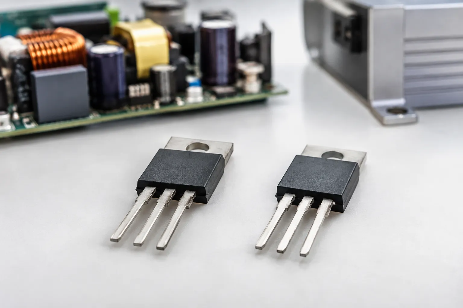
 7 Nov 2026
 7 min read
Silicon MOSFETs and silicon carbide MOSFETs use the same basic field-effect switching principle, but their semiconductor materials shape their voltage, switching, loss, and thermal characteristics. The difference between a Si MOSFET and a SiC MOSFET matters when matching a device to a converter’s operating conditions, package, and datasheet ratings. We supply SiC MOSFETs for engineers comparing device options; start by defining the electrical and mechanical requirements your design must meet.
Si MOSFET vs SiC MOSFET at a glance

A Si MOSFET uses silicon as its semiconductor material, while a SiC MOSFET uses silicon carbide; the practical choice depends on voltage, switching behavior, losses, cooling, and package requirements.
| Comparison criterion | Si MOSFET | SiC MOSFET |
|---|---|---|
| Semiconductor material | Silicon | Silicon carbide |
| Voltage and operating point | Assess the device’s rated limits against the circuit’s voltage and transients. | Assess the device’s rated limits against the circuit’s voltage and transients. |
| Switching behavior | Compare switching characteristics with the intended frequency and gate-drive conditions. | Compare switching characteristics with the intended frequency and gate-drive conditions. |
| Losses | Calculate conduction and switching losses at the actual operating point. | Calculate conduction and switching losses at the actual operating point. |
| Thermal design | Check power dissipation, thermal resistance, and the available cooling path. | Check power dissipation, thermal resistance, and the available cooling path. |
| Packaging | Choose a package compatible with board layout and cooling. | Choose a package compatible with board layout and cooling. |
This table compares device categories, not particular parts: the datasheet determines the ratings and behavior of an individual device. To compare SiC devices for a specific design, start with the SiC MOSFET range, then check the part-level data against your requirements.
A discrete MOSFET is not the same thing as a SiC MOSFET module. A module integrates devices in a package, so selection also involves how the module fits the converter’s electrical, thermal, and mechanical design.
How Si and SiC MOSFETs differ in material and structure

Both types control current through a MOSFET gate structure, but the semiconductor material differs: silicon is used in Si MOSFETs, and silicon carbide is used in SiC MOSFETs.
In either device, the gate voltage controls a conductive channel between the device’s main terminals. Applying an appropriate gate-to-source voltage turns the channel on; changing the gate voltage turns it off. The circuit designer uses that controlled switching to regulate current in a power-conversion stage.
The material affects the device’s electrical characteristics, but the label alone does not specify how a particular MOSFET will behave. Relevant details include rated voltage, on-state resistance, gate-charge and switching characteristics, and thermal ratings. These are device-level parameters: compare values under equivalent conditions and use the datasheet’s stated test conditions rather than relying on a technology name as a performance guarantee.
For a SiC MOSFET, the device’s body-diode behavior and gate-drive conditions also matter to circuit design. A relevant reliability-test method evaluates changes in on-state voltage, on-state resistance, and reverse drain voltage due to body-diode operation; the IEC SiC MOSFET test method describes that scope. It is a test-method reference, not a substitute for the individual device’s ratings or application guidance.
The same selection discipline applies when looking for a silicon device. Compare the stated electrical ratings and package against the design rather than assuming that every Si MOSFET will suit a given voltage or switching task. Quest Semi also lists silicon MOSFET devices for readers assessing that device category.
How voltage ratings and switching behavior compare
Voltage rating and switching behavior must be assessed for the actual circuit: neither silicon material nor a nominal rating alone proves that a device fits an application.
Start with the maximum operating voltage and the conditions that can produce transients. The device’s voltage rating must be evaluated against the circuit’s voltage stress, including the effects of switching and the implementation. Leave room for the design’s required operating margin according to the applicable design criteria; do not treat a nominal device rating as a target operating voltage.
Next, consider switching frequency and the transition behavior required by the converter. Switching faster can change switching losses, voltage and current waveforms, and electromagnetic interference. The practical result depends on the device, gate drive, circuit layout, and operating point. A SiC MOSFET is not a drop-in performance guarantee: its datasheet’s gate-drive guidance and switching parameters must be considered with the surrounding circuit.
Replacing a Si MOSFET with a SiC MOSFET therefore calls for more than checking the new device’s voltage rating. Review the gate driver, gate resistance, switching waveforms, voltage overshoot, protection behavior, and thermal conditions. Confirm that the device’s ratings and recommended operating conditions match the design. If the new device changes switching transitions, reassess layout and electromagnetic compatibility rather than assuming the original implementation remains suitable.
For a module, assess the integration details as well as the semiconductor characteristics. The module’s terminals, package, cooling interfaces, and electrical configuration affect how it connects to the converter. The module integration and selection guide focuses on those additional considerations.
How losses, thermal design, and packaging affect performance
Device losses depend on operating conditions, and the resulting heat must be managed through a package and cooling path that fit the application.
Conduction and switching losses
Conduction loss occurs while the device carries current in its on-state; switching loss occurs during transitions between on and off states. Both need to be estimated at the design’s intended current, voltage, switching frequency, and temperature.
For a first-order conduction comparison, on-state resistance is a key datasheet value for a MOSFET. Its effect depends on current and operating temperature, so a room-temperature resistance value alone does not settle the comparison. Check how the datasheet specifies resistance and consider the device’s thermal operating conditions.
Switching loss depends on how voltage and current overlap during transitions and how often those transitions occur. Compare switching data under relevant test conditions, then account for the intended gate drive and circuit implementation. A device with a potentially useful switching characteristic in one setup may not produce the same system-level outcome in another.
Avoid selecting by one loss figure in isolation. Estimate conduction and switching contributions over the expected operating range, then check whether the combined dissipation is manageable in the actual thermal design. If the comparison involves a SiC MOSFET module, use module-level documentation as well as device-level information; integration can change the thermal and electrical context.
Thermal and package considerations
Thermal performance depends on device dissipation, the path from the junction to the cooling system, and the package’s stated thermal characteristics.
Begin with the datasheet’s maximum junction temperature and thermal-resistance information, then identify the design’s cooling method and ambient conditions. Use the relevant thermal path for the package and mounting arrangement. A device’s material does not by itself establish that the design will run cooler: the result depends on losses, thermal interfaces, heatsinking, airflow or other cooling, and the system’s operating conditions.
Package constraints affect both thermal management and electrical implementation. Check package dimensions, pinout, mounting needs, creepage and clearance requirements where applicable, and compatibility with the board or busbar. Also consider the current path and parasitic inductance: layout and connection geometry can influence switching behavior and voltage overshoot.
For a discrete device, confirm that the available package matches the design’s mechanical envelope and cooling approach. For a module, review its mechanical outline, electrical connections, and prescribed thermal interface. A smaller package is not automatically a better fit if it cannot meet the cooling or interconnection requirements.
Choose the MOSFET that fits your operating conditions

Choose between Si and SiC by matching each candidate’s datasheet ratings and package to the circuit’s voltage, switching, loss, thermal, and mechanical requirements.
Use the same evaluation conditions for both device types. A useful comparison records the circuit’s operating voltage and transient expectations, required current, switching frequency, gate-drive constraints, estimated losses, cooling method, and available package space. Then compare each candidate’s ratings and test conditions against those requirements.
A specific request such as “1700 V, 160 mΩ, TO-247” is a set of distinct constraints, not a general request for a high-voltage SiC MOSFET. Check whether the candidate’s voltage rating, on-state resistance, and package each match the stated requirement. If one value does not match, do not treat the part as equivalent simply because another specification is close. Confirm other necessary characteristics in the datasheet before considering it for the design.
The same rule applies when comparing technologies: SiC may be worth evaluating where its device characteristics align with the application, but it is not automatically the right choice for every converter. A Si MOSFET may be the appropriate option when its ratings and performance satisfy the requirements. The decision should follow from the operating point and implementation, not from a blanket preference for one material.
Before committing a design, have a qualified power-electronics professional review the component choice and system-level implications for the specific application.
Recommended next steps
Move from a technology comparison to a device decision by turning the application requirements into a short, checkable set of electrical and mechanical criteria.
- Record the converter’s operating voltage, expected transients, current, switching frequency, and gate-drive limits.
- Define the required on-state resistance, thermal limits, cooling method, and package constraints.
- Compare candidate datasheets under comparable test conditions, including ratings, switching parameters, and thermal information.
- Reassess the gate driver, layout, protection, and thermal design if replacing a Si MOSFET with a SiC MOSFET.
- Review available SiC MOSFETs against the requirements, and confirm every required rating and package detail in the relevant product information.
Explore SiC MOSFETs
Compare the listed SiC MOSFET options with your required voltage, resistance, and package, then use the device information to assess fit.
