
Blog
Inside the SiC MOSFET structure


 28 Oct 2026
 5 min read
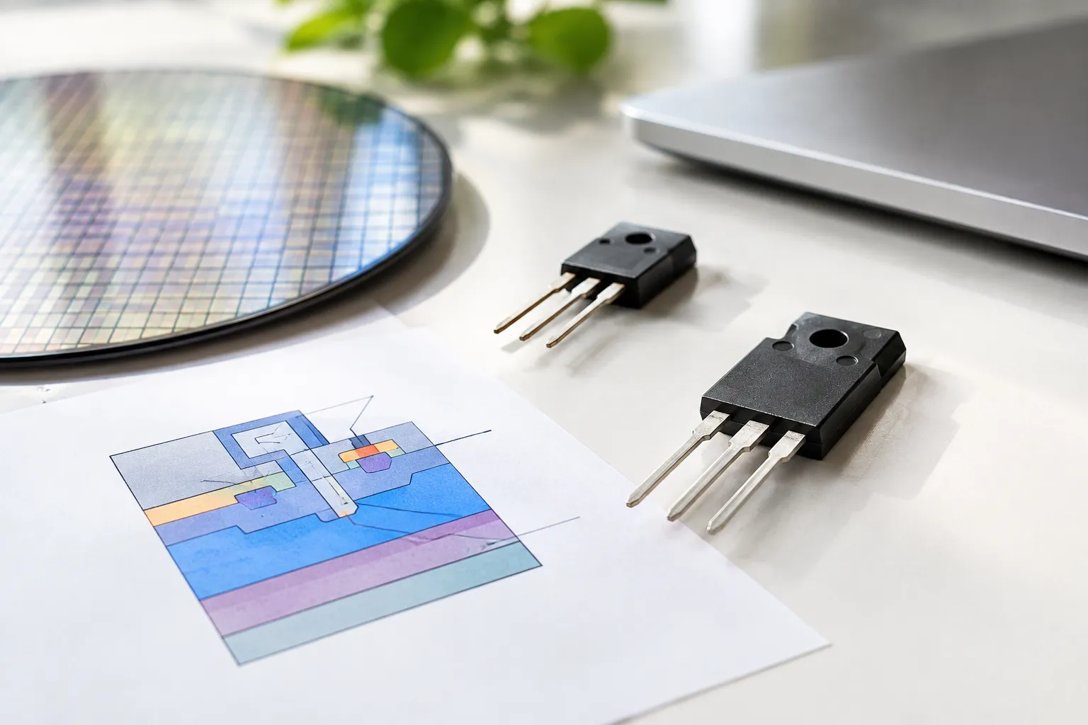
A SiC MOSFET is a vertical power switch built from silicon carbide layers. Its structure includes a substrate and drift region for voltage blocking, a body and source region, and an insulated gate that controls a surface channel. The cell layout and doping determine how those parts work together; the circuit symbol does not show the internal design.
The layers inside a SiC MOSFET

In a typical vertical n-channel SiC MOSFET, current travels between the top-side source and the backside drain. The main structural elements are:
- Substrate: A relatively heavily doped SiC base that supports the device layers and provides a conductive path to the drain contact.
- Drift region: A more lightly doped layer above the substrate. It supports much of the applied voltage when the MOSFET is off.
- Body region: A p-type region formed within the drift layer. It separates the source from the drift region until the gate creates a channel.
- Source region: A heavily doped n-type region within the body. It connects to the source terminal.
- Gate oxide: An insulating layer between the gate electrode and the SiC surface. It allows the gate’s electric field to control the surface without a direct conductive connection.
- Gate: The electrode that controls whether an inversion channel forms in the body region.
The body is usually electrically connected to the source in a power MOSFET. That connection affects the body junctions and helps prevent the body potential from floating during operation. Exact cell geometry and layer dimensions vary by device; a general diagram explains the device physics, not the construction of every part.
The same material family also appears in other power components. For example, High Voltage Silicon Carbide Diodes use SiC for a different device structure and switching function.
How planar and trench cells arrange the gate

The gate’s position relative to the body region defines the cell layout. Two common approaches are planar and trench.
In a planar cell, the gate sits over the surface of the device. The channel forms along the surface of the body region, beneath the gate oxide. This layout keeps the gate structure at the top surface.
In a trench cell, the gate occupies a groove etched into the SiC. The channel forms along a sidewall of that trench, where the gate is insulated from the surrounding semiconductor. This changes how cells can be arranged and how much channel area can fit within a given footprint.
Neither layout is automatically the right choice for every application. The design tradeoffs depend on the device implementation and its electrical and thermal limits. When comparing parts, use the datasheet’s specified ratings and characteristics rather than inferring performance from the word “planar” or “trench” alone. For related switching considerations, see our guide to SiC MOSFET switching benefits and tradeoffs.
How the gate forms a conducting channel

For a typical n-channel enhancement-mode SiC MOSFET, applying a sufficiently positive gate-to-source voltage creates an electric field across the gate oxide. That field attracts electrons to the surface of the p-type body beneath the gate, forming an inversion channel.
The channel connects the n-type source region to the n-type drift region. With the drain at a higher potential than the source, this provides a controlled path through the vertical device. Removing the gate drive lets the channel disappear, interrupting that controlled path.
The required gate voltage and the allowed operating range are device-specific. Threshold voltage is not a recommended drive voltage: it describes the onset of conduction under stated test conditions, not necessarily the voltage needed to achieve a particular on-state resistance. Read the gate-drive limits and test conditions in the specific datasheet. For a broader explanation of the underlying device category, see what a power MOSFET is.
How the drift region blocks voltage when the device is off
When the channel is absent, the p-type body and n-type drift region form a junction. Under off-state drain voltage, the depletion region extends into the drift region, which supports much of the voltage between the drain and source.
The drift region’s doping and thickness are design variables: they affect voltage blocking as well as conduction characteristics. This is why the internal vertical structure matters to the device’s ratings, but it does not provide enough information on its own to select a part. The datasheet’s voltage ratings and operating conditions remain essential.
Relate the internal structure to the circuit symbol
A SiC MOSFET symbol shows the device’s circuit connections and switching function. For a common discrete n-channel device, it identifies the gate, drain, and source terminals; the body diode is often represented as well.
The symbol is a circuit-level shorthand, not a cross-section. It does not show the substrate, drift layer, gate oxide, or whether the cells use a planar or trench arrangement. Nor does it specify voltage rating, on-resistance, package, or gate-drive limits. Those details belong in the part’s documentation.
SiC MOSFET Structure FAQ
What is the structure of SiC?
A typical vertical SiC MOSFET has a substrate, a voltage-supporting drift region, a p-type body, an n-type source, and an insulated gate. The gate controls a channel in the body region.
What is the difference between a Si MOSFET and a SiC MOSFET?
Both use an insulated gate to control a channel, but one uses silicon and the other silicon carbide as the semiconductor material. Their material properties and device implementations affect ratings and switching behavior, so compare specific datasheets for an application.
Use the structure to assess device datasheets
The structure provides a framework for reading specifications, but it cannot replace them. When assessing a SiC MOSFET, check:
- Drain-to-source voltage rating and the conditions attached to it.
- On-resistance, including its stated gate voltage and temperature.
- Gate threshold and recommended gate-drive range.
- Switching and capacitance data under their specified test conditions.
- Body-diode characteristics and any stated operating limits.
- Package, pinout, thermal information, and mounting requirements.
For a request such as a particular voltage rating, resistance, and TO-247 package, verify each requirement against the same device’s datasheet. A matching voltage rating alone does not establish a match for resistance, package, or operating conditions. The internal structure explains why those specifications matter; the datasheet determines whether a specific component meets the design requirements.
Irina Kulkarni writes about power semiconductor technologies and their role in efficient power conversion. She has a background in electrical engineering and experience evaluating silicon carbide devices for high-voltage applications. Her coverage includes SiC diodes, MOSFETs, device selection, and practical design considerations for engineers working on EV, renewable energy, and data centre systems. She aims to make technical guidance precise, useful, and grounded in real design trade-offs.
